



IBM’s Announces 0.7nm Process Node, Introduces NanoStack
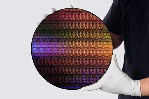
There’s a reason why I keep asking high-profile executives and architects at major semiconductor companies about whether they think Moore’s Law, the process of improving transistor density*, is still in the works. On the one hand we’ve got Jensen at NVIDIA saying that Moore’s Law is dead, joined in part by Huawei but only simply because of not having access to the latest tools. On the other are AMD and Intel who recognise that Moore’s Law is part of the ongoing evolution and still remains a critical part. In the middle is TSMC, who in the words of Deputy Co-COO Kevin Zhang, told me ‘I don’t care.’ So who is correct? When it comes to IBM, I firmly believe they’re in the camp of saying Moore’s Law is still alive. Four years ago, in 2021, the company announced it was the first to achieve a scaled Gate-All-Around (GAA) transistor design in a number of test vehicles between full logic and memory designs. This was substantial, as Gate-All-Around technology had been earmarked as the next stage beyond the FinFET designs that are common in the industry since 2012. IBM referenced the technology as a ‘2nm-class’ design, and while the only direct licensee of its technology is Rapidus in Japan, it paved the way for a wealth of Gate-All-Around designs to start hitting the market this year, in fact. While TSMC, Intel, and Samsung developed their own equivalents, IBM was proud to announce itself as the first. Fast forward to 2026, and IBM is set to do it again. The transistor roadmaps from the leading research houses (eg imec) have earmarked that beyond several generations of FinFET then several generations of Gate-All-Around designs, the industry would pivot to a new design called CFET, or Complimentary FET. Instead of scaling transistors across a chip in a two dimensional way, CFETs enable a form of stacking, enabling more transistors in the x/y plane. There are multiple types of CFET design in the literature, and specifically IBM has built a staggered sequential CFET design . More on that later in the article. IBM has dubbed its new technology with a marketing term: NanoStack . The baseline numbers look kind of mindboggling, similar to what we saw with the move from FinFET to GAA. 50% Logic Area Scaling 50% Performance at iso-power 70% Efficiency at iso-performance 40% SRAM scaling 666 Million Transistors per Square Millimeter (666 MTr/mm 2 ) * In these numbers, IBM is compared to its own 2nm process technology. *The 666 number comes from IBM’s press release that states ‘100 billion transistors in the size of a fingernail’. IBM said half that number in a fingernail for its previous 2nm, and we got clarification they meant approx 150mm 2 . So 100 BTr / 150 mm 2 = 666.66 MTr/mm 2 . There’s a better number later in the article. IBM expects the scaling of the process to take around five years before this technology hits the market. IBM stated that the ‘expected markets who can take benefit’ of the technology would likely adopt it first, and based on current macroeconomics and chip design methodology, that’s still likely to be smartphone or small AI chiplets. Thanks for reading More Than Moore! This post is public so feel free to share it. Share The company also states that this technology would benefit from High-NA EUV to reduce the number of patterning steps on critical layers. However it should be noted that it isn’t technically needed - IBM is currently in the process of waiting for the High-NA EUV tool at Albany NanoTech to be installed and they’ll use that. In the rest of this article, we’ll go into the details we know about the technology, as well as some pre-amble to ensure we’re all on the right level. One of the best ways to understand what’s coming down the pipeline from the big players in terms of transistor design is to look at what’s happening in the research conferences and from the research institutions. Over the last decade leading up to the productization of the latest transistor technology, there are lots of research papers and presentations about work being done to build and develop what’s in the roadmap. What is in the roadmap? Well it up to now the transistors have gone through this. Source: Lam Research On the left is the Planar transistor, which was the main method for building transistors all the way up until the 2010s. It still is the base design for all chips built at 22nm and above, and is comparatively the simplest design, however it is the reason for a lot of advancements in this space. As we shrink a planar transistor to fit more on a chip, if we shrink them too much then the source and drain become too close causing electrons to leak, and the design reaching electrostatic limits as they shrank. The FinFET transistor in the middle solved that issue. By extracting the source and drain up out of the substrate and wrapping the gate around it, this lead to better electrostatic control and conducting channels on three sides, rather than just the one. This leads to an increase in drive current for higher performance. Multiple generations of FinFET shrank the design but increased the height of the fins, to maintain balance. As scaling continues, tall fins become fragile to manufacture and the ‘fourth’ side of the fin without a gate is overpowered by the electric field. Not only that, but another way to increase density was through fin depopulation, using only one or two fins per transistor, which reduces drive current and switching speed. This led to the Gate-All-Around design. By wrapping the gate all the way around the channel, the result is better control and current flow. Instead of ‘fin depopulation’, designers can control the number of layers in their gate, as well as the gate width, in order to fine tune the performance and power needed for a given cell or cell library. The complexity of gate-all-around comes from the need to build the layers or ‘sheets’ - while they look simple enough in this diagram, each one needs to be surrounded by a protective layer, and the steps to do that rely on some interesting chemistry and physics. The sheets themselves may only be five nanometers thick (so, 15 atoms) with a few atoms of protective layer, but the sheets often vary between 20 and 40 nanometers in width. In the design phase of Gate-All-Around, we saw a wild array of approaches from the main players and research houses. Firstly around getting it to work in the first place, then designs from 2 sheets up to 7 sheets, with the materials and spacing being fine tuned. The first GAA silicon is now currently on the market as of late 2025, with: Intel is using a four layer design branded ‘RibbonFET’ in its 18A process node technology (Clearwater Forest, Panther Lake, Wildcat Lake). TSMC is implementing GAA in its N2 node using three sheets, with the first product expected to hit the market later this year with AMD and its new CPU, Venice (more on that at the end of August at their AI day). Samsung would argue they were the first to market with GAA in their 3nm design process SF3E in 2022, with a crypto ASIC for MicroBT. Their first mainstream product with GAA on SF2 was the Exynos 2600 mobile processor in late 2025. Rapidus has licensed IBM’s technology design and is currently installing tools in its new 2nm fab in Chitose, Hokkaido. It has already started running test wafers since 2025, with first product tapeouts in late 2026 and production ramp through 2027. Here is imec’s roadmap from 2023. The process node names are a little behind, but it represents a key feature of modern semiconductor technology development. From N7 to N3, imec highlights three generations of FinFET technology, with one of the main dimensions being metal pitch scaling. From N3 to N2, we have the transition from the latest generation FinFET to the first generation of Gate-All-Around with nanosheets. N2, A14, A10 and A7 are all generations of Gate-All-Around design. When we hit A10 in this roadmap, the gap between consecutive NFET and PFET gets replaced by a barrier to enable them to be closer together - this has been dubbed ‘ForkSheet’ in the literature but most players now just call it an updated version of GAA. Then we move into CFETs. The point here is to show that each fundamental transistor design is built with several generations in mind, allowing for low hanging fruit improvements before a big pivot to something potentially a lot harder, with a lot more steps, or simply because the research hasn’t been done or the material science needs to happen. It takes a long time to do any of these steps, and hundreds of thousands of people. Not only the transistors but power delivery, metal stack design, and everything else. It means that when I show this image above, each one of these steps can be seen as a multi-generational effort, and not simply one after the other. CFET also comes in a variety of designs, has its own multi-generational effort, eventually leading to 2D transistors using Transition Metal Dichalcogenides (TMDs) like molybdenum disulphide (MoS 2 ) and tungsten diselenide (WSe 2 ). We’re expecting that announcement in 2031. That was a joke. On the face of it, given the image above, a CFET looks like a silicon designer’s dream. Overnight, it’s an immediate doubling of density compared to GAA. IMMEDIATE. I mean, look at that diagram - since whenever has a diagram been misleading? Let’s start by mentioning at least some of the research that has led up to CFET. Technically by the definition of NMOS over PMOS as in the diagram, it’s not always necessary that the two parts have to be GAA, i.e. GAA on GAA. Over the last five years we’ve seen research from Intel and others showing one Fin on one sheet of GAA, Fin on Fin, and maybe even planar in the mix. That’s simply because planar and fin are well known processes. A lot of this research was also done at larger nodes too. Source: TSMC 1-on-1 mCFET with MDI, 2024 However in the last 3 years or so, we’ve seen more efforts for two-sheet GAA on top of two-sheet GAA, and the evolution of that. Ultimately production level CFETs are expected to be 3-on-3 or 4-on-4 or a mix in between. But truth be told, there are two main ways that the industry has been looking at even building these designs. We call them monolithic CFET and sequential CFET . Source: ETRI Monolithic CFETs ( mCFET ) have a clue in the name. Much like a multi-sheet GAA design, a monolithic CFET will build all six to eight layers on one piece of silicon, then do the etching/plating/filling as necessary. There’s some additional control needed to enable that, but broadly speaking it’s as complex as building more layers onto a GAA design. The top line benefits of such an approach are meant to be simplicity and density. A lot of work is being placed into mCFETs to ensure performance, yield, and scale. One of the main issues is the restriction on process steps as the stack is built higher. Because pMOS and nMOS have different materials that build them, any step to build the nMOS on top of the pMOS (and vice versa) cannot interfere with what is underneath. So you can forget that 1400oC annealing step and spend years trying to research a new way that is as good, as cheap, and as scalable. Sequential CFETs ( sCFET ) instead bond together using two or more wafers. That’s a relatively easy way of looking at it, but there are multiple methods. One, each wafer has a set of GAA devices on them, either all nMOS or all pMOS, and with some clever physics, are bonded together such that they connect in the right places with the right overlay and act like a CMOS transistor pair. The benefit of such a design means that each type of transistor can be heavily optimized without worrying about the effect on the other - even more so than a traditional GAA or FinFET design. Two, the first wafer has a set of GAA devices on them, and the second carrier wafer brings over some structures for the upper tier and the rest of the design is fabricated on top. This is a stop gap to assist with specific device optimisation, but still needs careful planning to deal with thermal integration as mentioned above. The downside is the bonding - it has capacitance and a margin of error, and any slight deviation makes both a lot worse. Modified from source: imec There’s an interesting discussion as to which process might be more expensive. On the one hand, mono-CFETs have additional layers on the same wafer, leading to cascading yield metrics on a single piece of silicon. By contrast, sCFETs can only need half the number of sheets on each wafer, but the cost comes from the bonding accuracy and yield loss. In the diagram above, imec is showing three generations of sCFETs and how the bonding between them evolves. Which one of the two is better is hard to say, and will depend long term based on the research. Again, if we’re looking at 2031 for the first CFET designs to hit the market (we still have 3-4 generations of GAA first), then how those designs are improved and research will determine which ends up better. An old report from SemiAnalysis in 2024 claimed that all the leading fabs were primarily looking at mCFETs. Instead, IBM is going down a third route. It has been known for a while that NMOS and PMOS transistors prefer different orientations of silicon atoms. If you’re wondering how silicon has different orientations, it’s all to do with the lattice inside and if you were to cut it in a specific direction, where exactly you would cut it. The green lines are where you would cut an infinitely repeating crystal. So on the left, a cut into silicon in the (001) plane would give you five atoms in red direct, whereas in the (110) would give you eight atoms in red. You can cut in any plane, such as (010) or (101) or (011), but these are the two that matter in this context. It turns out that for transistor performance, NMOS transistors prefer (001), and PMOS prefer (110). What this means is the “mobility of the conducting element” in each transistor type is improved by the different silicon orientation. If you’re also wondering why I worded it that way and didn’t simply say mobility of electrons, it’s because NMOS uses electrons but PMOS uses electron holes. It’s a material science thing that works, and the mobility of each matters, but is beyond the scope of this article. The problem with needing two different silicon orientations is that in a monolithic design, you are limited to one or the other, at least in planar and FinFET transistors. You could technically grow silicon ep
Source: More Than Moore